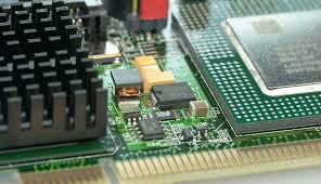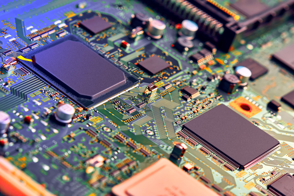
Introduction to Physical Design Training Institutes in Bengaluru
Are you ready to take your career in physical design to the next level? Look no further than the vibrant city of Bengaluru, India’s Silicon Valley. With a booming tech industry and many opportunities waiting to be seized, Bengaluru is home to top-notch Physical Design Training Institutes that can help you excel in this dynamic field. Join us on a journey from novice to expert as we explore how these institutes can shape your future in semiconductor technology.
Benefits of Enrolling in a Physical Design Training Institute
Embarking to excel in physical design can be challenging and rewarding. Enrolling in a Physical Design Training Institute in Bengaluru opens doors to a world of opportunities that can shape your career trajectory.
One of the key benefits is gaining access to expert faculty who bring years of industry experience and knowledge to the classroom. Their guidance and mentorship can provide invaluable insights into the latest trends and technologies shaping the field.
Additionally, these training institutes offer specialized courses tailored to equip students with practical skills sought after by top companies in the semiconductor industry. From learning about advanced placement techniques to mastering timing closure, the curriculum is designed to bridge the gap between theoretical concepts and real-world applications.
Moreover, being part of a Physical Design Training Institute allows students to network with like-minded peers and establish connections within the industry. This exposure can lead to internships, projects, and job placements at leading semiconductor companies upon graduation.
Curriculum and Courses Offered by Physical Design Training Institutes in Bengaluru
Choosing the right training institute is crucial when pursuing a career in physical design. In Bengaluru, Semicon Technolabs stands out for its comprehensive curriculum and diverse courses tailored to meet industry demands.
The curriculum at Semicon Technolabs covers a wide range of topics, including VLSI design, placement and routing techniques, clock tree synthesis, power analysis, and more. Students get hands-on experience with industry-standard tools like Cadence Virtuoso and Synopsys IC Compiler.
Courses offered include foundational modules on digital electronics and CMOS design, followed by advanced subjects such as physical verification and signal integrity. Additionally, students can opt for specialization tracks in areas like analog layout or FPGA design to further enhance their skills.
With a blend of theoretical knowledge and practical exposure, graduates from Semicon Technolabs are well-equipped to excel in the semiconductor industry’s competitive field of physical design.
Faculty and Teaching Methodologies at Physical Design Training Institutes
One critical factor that sets Physical Design Training Institutes in Bengaluru apart is their exceptional faculty members. These institutes boast a team of experienced professionals who bring real-world expertise to the classroom.
The teaching methodologies are practical and hands-on, allowing students to gain valuable skills through interactive learning experiences. Faculty members go above and beyond to ensure that each student receives personalized attention and support throughout their training.
With a focus on industry-relevant curricula and cutting-edge technologies, these institutes prepare students for the dynamic field of physical design. The faculty’s dedication to excellence helps students develop a deep understanding of concepts and challenges them to think critically.
By learning from industry experts, students acquire technical knowledge and gain insights into current trends and best practices in physical design. This exposure equips graduates with the tools they need to excel in their careers upon completing the program.
Industry Connections and Job Opportunities for Graduates
Regarding excelling in physical design, having strong industry connections can open up opportunities for graduates from training institutes in Bengaluru. These connections bridge academia and real-world applications, providing students with insights into current trends and technologies.
Physical design training institutes often collaborate with leading companies in the semiconductor industry, offering students valuable networking opportunities through guest lectures, workshops, and internships. By interacting closely with industry professionals, graduates can gain practical knowledge and hands-on experience that are highly sought after by employers.
Moreover, these connections can lead to potential job placements upon graduation. Many companies actively recruit talent from physical design training institutes in Bengaluru due to their specialized curriculum and focus on industry-relevant skills. This direct link between education and employment enhances the employability of graduates and accelerates their career growth within the semiconductor sector.
By leveraging these industry connections nurtured by physical design training institutes in Bengaluru, graduates can pave the way for a successful career path in this dynamic and competitive field.
Success Stories from Alumni of Physical Design Training Institutes
Imagine stepping into the shoes of successful alums from Physical Design Training Institutes in Bengaluru. Picture yourself as they recount their journey from novices to experts in the industry, all thanks to the specialized training they received.
These alumni share how their skills were honed through hands-on projects, expert guidance, and real-world simulations that prepared them for the challenges of the semiconductor industry. They talk about overcoming obstacles, pushing boundaries, and achieving milestones they once thought were out of reach.
From securing coveted positions at top companies to leading innovative projects, these success stories inspire current students to dream big and work hard. The alumni emphasize the importance of perseverance, continuous learning, and staying updated with cutting-edge technologies in physical design.
Their experiences testify to the transformative power of quality education and practical training offered by Physical Design Training Institutes in Bengaluru.
Conclusion: Why Choosing a Physical Design Training Institute in Bengaluru Can Be the Key to Your Success in the Industry
Choosing a Physical Design Training Institute in Bengaluru, such as Semicon Technolabs, can be the key to unlocking your potential and excelling in the industry. With a comprehensive curriculum tailored to industry standards, experienced faculty members, and strong connections with leading companies, these institutes provide you with all the tools you need to succeed.
By enrolling in a physical design training institute in Bengaluru, you gain valuable knowledge and skills and open doors to endless opportunities for growth and success. The success stories of alumni who have secured promising careers serve as testaments to the quality of education these institutes provide.
If you want to make your mark in physical design, consider investing in yourself by joining a reputable training institute. Your journey from novice to expert starts here – take that first step towards a rewarding career today!