Ranked Among the Top 10 Most Promising VLSI And Semiconductor Companies - SILICONINDIA
Best VLSI Training Institute in Bangalore & Hyderabad
Launch Your Career in
VLSI and Semiconductor with AI Integration
Master Design Verification, Physical Design, DFT, Analog Layout and Analog Circuit Design at the best VLSI training institute in Bengaluru & Hyderabad, with industry focused training from experienced mentors.
Build a successful semiconductor career through industry-focused
training, expert mentorship, hands-on projects, advanced EDA tools,
and dedicated placement support designed to make you job-ready.
Gain practical knowledge through hands-on learning, real-time VLSI design projects, and industry-focused training methodologies.
Industry-Oriented Training
Expert Mentors
Learn directly from experienced professionals working in leading semiconductor companies with real industry expertise.
Comprehensive VLSI Programs
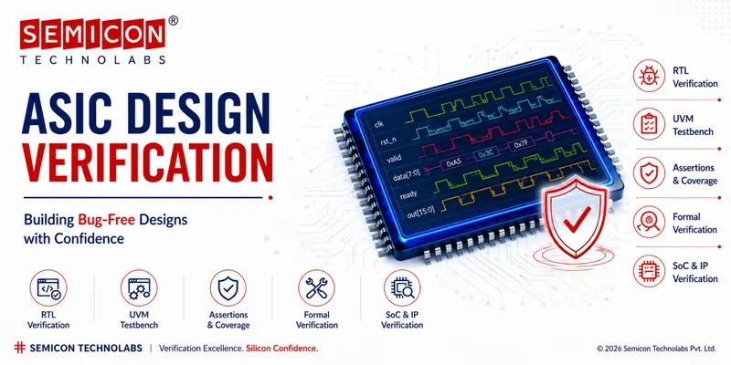
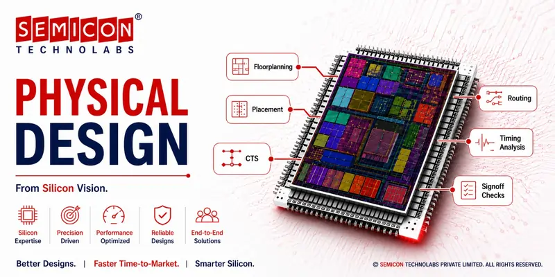
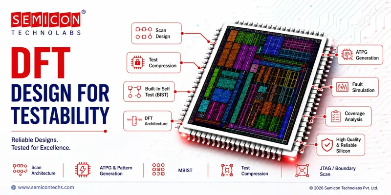
Master in Design Verification (DV), Physical Design (PD) Design for Test (DFT), Analog Layout (AL), and Analog Circuit Design (ACD).
Corporate Training Solutions
Customized corporate training programs designed to meet specific semiconductor industry skill requirements.
Hands-on EDA Tools
Work with industry-standard EDA tools and modern VLSI design methodologies used by top semiconductor companies.
Project-Based Learning
Develop practical skills by completing real-world semiconductor projects that strengthen your technical portfolio.
Industry-Ready Curriculum
Curriculum aligned with the latest semiconductor technologies, workflows, and current hiring requirements.
Career Support
Receive resume building, technical interview preparation, mock interviews, and career guidance from experts.
100% Placement Assistance
Dedicated placement support with industry connections to help you launch your semiconductor career.
Small Batch Sizes
Enjoy personalized mentoring, one-to-one attention, and better interaction with experienced trainers.
Proven Success
Trusted by aspiring engineers for successfully building rewarding careers in the global semiconductor industry.
Interactive VLSI Roadmap
Interactive VLSI Roadmap
See Your
Future
Before You Build It.
Every connection tells a story. Every domain unlocks
a new skill. Explore the complete VLSI ecosystem and
discover the path that matches your ambition in
semiconductor design.
Register Transfer Level
Verilog HDL
SystemVerilog
Digital Logic Design
RTL Coding
Finite State Machine (FSM)
Combinational Logic
Sequential Logic
Synthesizable Design
02
Design Verification (DV)
Core Domain
Functional Verification
Verification Methodology
Testbench Development
Constrained Random Verification
Assertion-Based Verification
Functional Coverage
Verification Planning
Debugging Techniques
Verification Closure
03
FPGA Design
Core Domain
FPGA Prototyping
Hardware Description Language
Digital System Implementation
Embedded Systems
FPGA Architecture
Hardware Acceleration
Real-Time Processing
FPGA Verification
FPGA Development
04
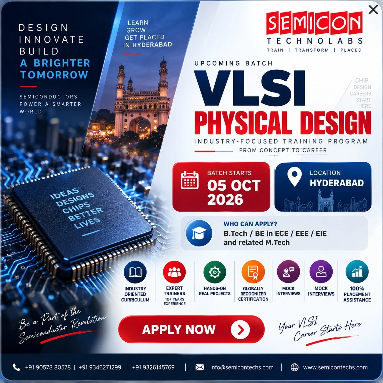
Physical Design (PD)
Core Domain
ASIC Physical Design
Floorplanning
Power Planning
Standard Cell Placement
Clock Tree Synthesis
Signal Routing
Physical Verification
Chip Implementation
Physical Design
GDS-II Generation
05
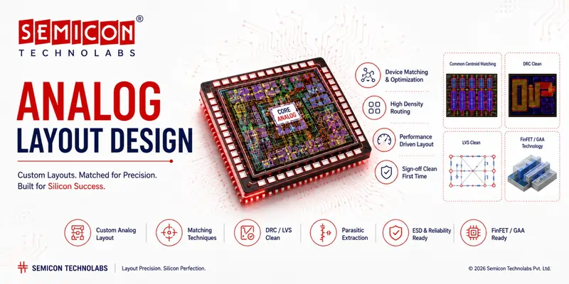
Analog Layout Design (ALD)
Core Domain
Full-Custom Layout
Layout Matching Techniques
Common Centroid Layout
Interdigitated Layout
Layout Versus Schematic (LVS)
Design Rule Check (DRC)
Parasitic Extraction (PEX)
Custom IC Layout
Layout Optimization
06
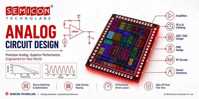
Analog Circuit Design (ACD)
Core Domain
CMOS Analog Design
Operational Amplifier Design
Current Mirrors
Voltage References
Phase Locked Loop (PLL)
Analog-to-Digital Converter (ADC)
Digital-to-Analog Converter (DAC)
Low-Power Analog Design
Mixed-Signal Design
07
Design for Test (DFT)
Core Domain
Scan Chain Insertion
Automatic Test Pattern Generation (ATPG)
Boundary Scan
Memory Built-In Self-Test (MBIST)
Logic Built-In Self-Test (LBIST)
Fault Simulation
Fault Coverage
Test Compression
Manufacturing Test
08
EMIR
Core Domain
Electromigration Analysis
IR Drop Analysis
Dynamic IR Analysis
Reliability Analysis
Power Grid Analysis
Current Density Analysis
Voltage Drop Analysis
Signoff Reliability
09
Static Timing Analysis (STA)
Core Domain
Timing Constraints
Setup Time Analysis
Hold Time Analysis
Timing Closure
Clock Domain Crossing (CDC)
Timing Optimization
Timing Signoff
On-Chip Variation (OCV)
Timing Verification
01
RTL Design
Core Domain
Register Transfer Level
Verilog HDL
SystemVerilog
Digital Logic Design
RTL Coding
Finite State Machine (FSM)
Combinational Logic
Sequential Logic
Synthesizable Design
02
Design Verification (DV)
Core Domain
Functional Verification
Verification Methodology
Testbench Development
Constrained Random Verification
Assertion-Based Verification
Functional Coverage
Verification Planning
Debugging Techniques
Verification Closure
03
FPGA Design
Core Domain
FPGA Prototyping
Hardware Description Language
Digital System Implementation
Embedded Systems
FPGA Architecture
Hardware Acceleration
Real-Time Processing
FPGA Verification
FPGA Development
04
Physical Design (PD)
Core Domain
ASIC Physical Design
Floorplanning
Power Planning
Standard Cell Placement
Clock Tree Synthesis
Signal Routing
Physical Verification
Chip Implementation
Physical Design
GDS-II Generation
05
Analog Layout Design (ALD)
Core Domain
Full-Custom Layout
Layout Matching Techniques
Common Centroid Layout
Interdigitated Layout
Layout Versus Schematic (LVS)
Design Rule Check (DRC)
Parasitic Extraction (PEX)
Custom IC Layout
Layout Optimization
06
Analog Circuit Design (ACD)
Core Domain
CMOS Analog Design
Operational Amplifier Design
Current Mirrors
Voltage References
Phase Locked Loop (PLL)
Analog-to-Digital Converter (ADC)
Digital-to-Analog Converter (DAC)
Low-Power Analog Design
Mixed-Signal Design
07
Design for Test (DFT)
Core Domain
Scan Chain Insertion
Automatic Test Pattern Generation (ATPG)
Boundary Scan
Memory Built-In Self-Test (MBIST)
Logic Built-In Self-Test (LBIST)
Fault Simulation
Fault Coverage
Test Compression
Manufacturing Test
08
EMIR
Core Domain
Electromigration Analysis
IR Drop Analysis
Dynamic IR Analysis
Reliability Analysis
Power Grid Analysis
Current Density Analysis
Voltage Drop Analysis
Signoff Reliability
09
Static Timing Analysis (STA)
Core Domain
Timing Constraints
Setup Time Analysis
Hold Time Analysis
Timing Closure
Clock Domain Crossing (CDC)
Timing Optimization
Timing Signoff
On-Chip Variation (OCV)
Timing Verification
Our Trainee's Success Story
YouTube Carousel
What Our Students Say About Semicon
Hear from our successful students who transformed their careers with our comprehensive VLSI training programs.
Semicon Technolabs - 5 Star Reviews
“
★★★★★
I recently completed the 4-month VLSI Physical Design
course at Semicon Technolabs. The course was
well-structured, practical, and easy to understand.
The trainers were knowledgeable, approachable, and
always ready to help. The hands-on training boosted
my confidence and technical skills.
B. Dinesh Reddy
VLSI Physical Design Student
Physical Design Course
“
★★★★★
Semicon Technolabs offers excellent VLSI and DFT
training with strong practical exposure. The
experienced faculty, industry-focused projects,
and placement assistance provide a solid foundation
for a successful career. The supportive learning
environment makes it a great place to learn
semiconductor technologies.
Sunil Maheshwaram
VLSI Training Student
VLSI & DFT Training
“
★★★★★
I successfully completed the Physical Design course
and had an excellent learning experience. The
curriculum balanced theory with practical tool-based
sessions, helping me gain confidence in
industry-standard VLSI workflows. I highly recommend
this course to anyone planning a career in VLSI.
Aditya Aditya
Physical Design Student
Physical Design Course
“
★★★★★
The VLSI Physical Design training at Semicon
Technolabs was highly effective. The trainers
provided excellent guidance, and the hands-on
experience with industry tools gave me a strong
understanding of Physical Design flows. A great
institute for aspiring VLSI professionals.
Sai Charan Gollagadda
VLSI Physical Design Student
Physical Design Course
“
★★★★★
I'm pursuing the VLSI Design Verification course
at Semicon Technolabs. The faculty explains
SystemVerilog, UVM, and simulation tools clearly.
The mentors are supportive, friendly, and always
available to solve doubts. I highly recommend this
institute for VLSI Design Verification training.
Vaahida Shaik
Design Verification Student
Design Verification Course
“
★★★★★
I had a great learning experience at Semicon
Technolabs. The instructors were knowledgeable and
supportive, and the ASIC Verification training
included valuable hands-on sessions. The institute
also provides 24/7 tool access, making it an
excellent choice for career growth.
Hemantha Chintalapudi
ASIC Verification Student
ASIC Verification Course
“
★★★★★
The “Silicon to Chip: 3-Day Hands-on VLSI Workshop”
at VIT-AP by Semicon Techno Labs was very informative
and practical. Hands-on Cadence tools exposure and
expert trainers made complex VLSI concepts easy to
understand.
Bharath Saieswar Goli
VLSI Workshop Participant
Silicon to Chip VLSI Workshop
“
★★★★★
I recently completed my VLSI Design Verification
(DV) training at Semicon Technolabs. The course
covered SystemVerilog, UVM methodology, and ASIC
Verification flow with hands-on practice using
industry-standard EDA tools.
Prasanna Kumar Duttagupta
VLSI Design Verification Student
Design Verification Course
“
★★★★★
Best institute to start a career in VLSI with
experienced industrial trainers. Great place to
learn and gain knowledge, with excellent placement
opportunities. I completed my DFT coaching and
got placed in CYIENT.