What Is Design for Test (DFT)? A Complete Guide
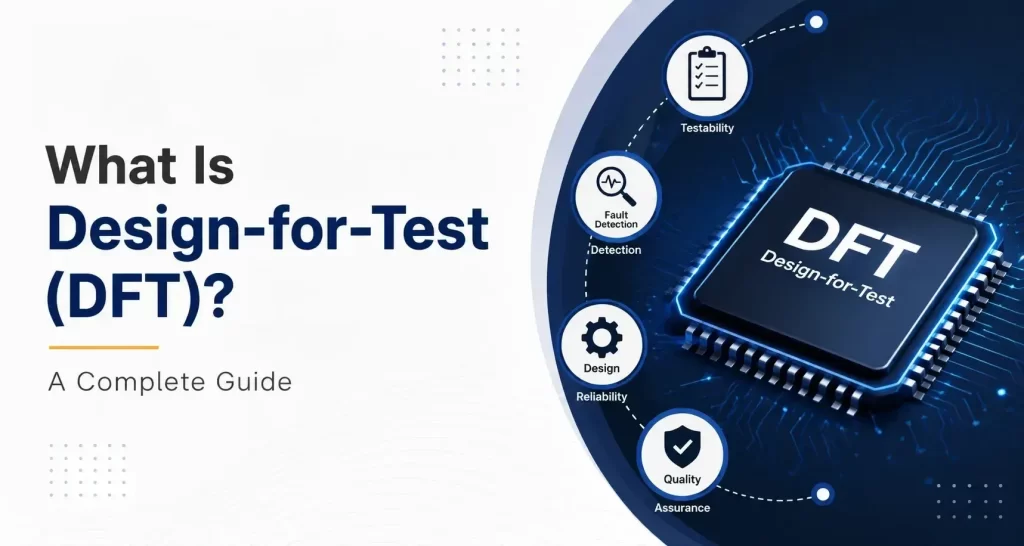
What Is Design for Test (DFT)?
What Is Design for Test (DFT)? It is one of the first questions every aspiring VLSI engineer asks, and the answer starts with a simple reality: modern semiconductor chips can contain billions of transistors and extremely complex logic. Designing the circuit is only one part of the semiconductor development process. Engineers must also ensure that the manufactured chip can be tested efficiently and that manufacturing defects can be detected with high confidence.
This is where Design for Testability (DFT) becomes essential.
Design for Test (DFT) is a semiconductor design methodology in which additional test structures and logic are incorporated into an integrated circuit during the design stage so that internal circuitry can be controlled and observed during manufacturing test.
In practical terms, DFT helps answer a critical question:
Once a chip has been manufactured, how can we efficiently determine whether the silicon is defect-free?
DFT techniques such as Scan Chain, Automatic Test Pattern Generation (ATPG), Built-In Self-Test (BIST), test compression, and Boundary Scan make it practical to test complex digital ICs and SoCs. These approaches are central to Modern IC Testing and VLSI Testing strategies used throughout the semiconductor industry.
For engineering students and professionals planning a career in semiconductor testing, DFT in VLSI is an important specialization with applications across processors, automotive SoCs, AI accelerators, networking chips, consumer electronics, and other high-volume semiconductor products.
What Is Design for Test (DFT)?
Design for Test (DFT), also called Design for Testability, is the process of adding dedicated test structures to an IC during the design phase to make the manufactured chip easier to test.
These structures are designed so that internal nodes and sequential elements become more controllable and observable during test mode.
During normal functional operation, the test structures generally remain transparent to the intended functional behavior. During manufacturing test, they provide mechanisms for:
- Controlling internal circuit states
- Observing internal circuit responses
- Applying test patterns
- Capturing circuit responses
- Detecting manufacturing defects
- Measuring fault coverage
- Supporting diagnosis and yield analysis
Simple Definition
DFT is the methodology of designing a semiconductor chip so that its internal circuitry can be efficiently tested after fabrication.
This is particularly important because physically probing every internal node of a modern SoC is impractical.
Why Is DFT Important in VLSI?
As semiconductor technology advances, ICs become larger, faster, and more complex.
A modern SoC may contain:
- Millions or billions of transistors
- Thousands of sequential elements
- Multiple clock domains
- Embedded memories
- High-speed interfaces
- Multiple power domains
- Analog and digital blocks
Testing such a chip only through its functional inputs and outputs would require an impractical number of test conditions.
DFT introduces additional test access mechanisms that improve controllability and observability.
Major Benefits of DFT
1. Higher Fault Coverage
DFT structures provide improved access to internal circuit elements, allowing ATPG tools to generate patterns for targeted fault models.
2. Reduced Test Complexity
Instead of relying exclusively on functional operation, scan-based methodologies provide direct access to sequential elements during test.
3. Reduced Manufacturing Test Cost
Efficient test architectures can reduce the number and duration of production test patterns.
4. Improved Product Quality
Effective DFT enables manufacturing defects to be detected before defective devices reach customers.
5. Better Diagnosis
DFT data can support fault diagnosis and help engineers identify likely locations or causes of failures.
6. Improved Manufacturing Yield Analysis
Test results provide valuable information for identifying systematic and random manufacturing issues.
7. Faster Time to Market
A robust DFT architecture can reduce the risk of discovering testability problems late in the chip development cycle.
DFT and the Semiconductor Manufacturing Process
DFT should not be viewed as an isolated activity performed only after RTL or physical design.
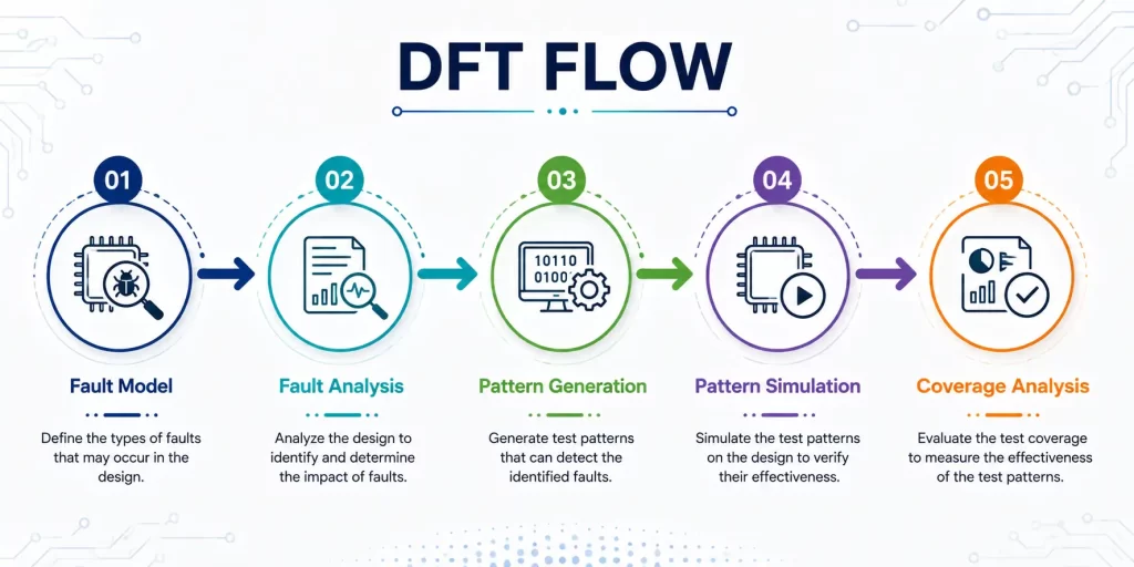
It interacts with several stages of the ASIC development flow and forms a critical part of the overall DFT flow followed across the industry.
A simplified flow is:
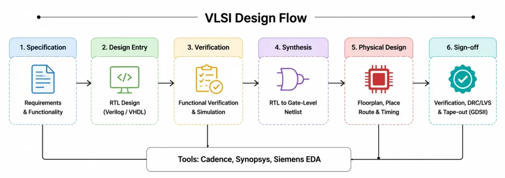
DFT engineers work closely with:
- RTL Design Engineers
- Design Verification Engineers
- Synthesis Engineers
- Physical Design Engineers
- STA Engineers
- Silicon Validation Engineers
- Test Engineers
This cross-functional nature makes DFT an important part of modern semiconductor engineering.
How Does DFT Work?
The fundamental idea behind DFT is to improve two properties:
Controllability
Controllability describes how easily a test system can force a particular internal circuit node or state element into a desired value.
Observability
Observability describes how easily the response of an internal circuit can be observed through available test outputs.
For a complex sequential circuit, both can be difficult to achieve using only functional inputs and outputs.
DFT structures improve these properties.
The most widely used approach for digital logic is scan-based DFT.
What Is a Scan Chain?
A Scan Chain connects scan-capable flip-flops into one or more serial shift registers.
In functional mode, these elements operate as normal flip-flops.
In test mode, they can be connected into scan chains.
A simplified scan sequence is:
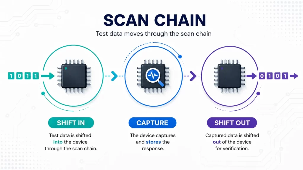
Shift In
A test pattern is serially shifted into the scan chain.
Capture
The circuit operates for the required test cycle and captures the response into the scan flip-flops.
Shift Out
The captured response is shifted out and compared with the expected response.
This architecture significantly improves access to internal sequential states.
IEEE technical references identify scan design as the most widely deployed DFT technique for logic testing.
What Is Scan Insertion?
During DFT implementation, selected functional flip-flops are replaced or configured as scan flip-flops.
These scan cells are then connected into scan chains.
A typical scan structure includes:
- Scan Input
- Scan Enable
- Scan Flip-Flops
- Scan Output
- Clock
- Test Control Signals
The exact architecture depends on the chip’s design and test requirements.
The objective is to provide sufficient internal controllability and observability while managing the impact on:
- Area
- Power
- Timing
- Routing
- Test time
What Is ATPG?
ATPG stands for Automatic Test Pattern Generation.
ATPG tools automatically generate test patterns designed to detect specific fault models.
Instead of engineers manually creating millions of test patterns, ATPG algorithms analyze the circuit and generate patterns that target faults efficiently.
Common fault models include:
- Stuck-at faults
- Transition faults
- Bridging faults
- Small-delay-related defects
Other technology- or methodology-specific fault models
Modern ATPG methodologies also consider factors such as test power, timing, compression, and diagnosis. Synopsys describes ATPG as a key mechanism used with DFT structures for detecting manufacturing defects and maximizing fault coverage.
What Are Stuck-at Faults?
A stuck-at fault model assumes that a signal line behaves as though it is permanently stuck at either logic:
0
1
For example:
SA0 → signal behaves as permanently 0
SA1 → signal behaves as permanently 1
ATPG attempts to generate input conditions that:
Activate the fault.
Propagate its effect to an observable point.
Detect the resulting response.
This is one of the fundamental concepts that every aspiring DFT engineer should understand.
What Are Transition Faults?
A transition fault model focuses on whether a signal can transition sufficiently fast between logic states.
Two common concepts are:
- Slow-to-Rise
- Slow-to-Fall
Transition testing becomes particularly important as operating frequencies increase and timing-related manufacturing defects become more significant.
What Is Fault Coverage?
Fault coverage is a measure of how effectively the generated test patterns detect the faults included in the selected fault model.
A simplified representation is:
Fault Coverage = Detected Faults / Testable Faults × 100
Higher fault coverage is generally desirable, but achieving high coverage is not simply a matter of generating more patterns.
Engineers must also consider:
- Untestable faults
- Redundant logic
- Pattern count
- Test application time
- Test power
- Compression
- Diagnosis requirements
Therefore, DFT optimization is a multi-dimensional engineering problem.
What Is Test Compression?
Large SoCs can contain extremely long scan chains and potentially large ATPG pattern volumes.
Test compression reduces the amount of test data that must be stored and transferred while maintaining effective fault coverage.
Compression architectures may use:
- On-chip decompression
- Response compaction
- Multiple internal scan chains
- Compact test interfaces
The goal is to reduce:
- Test data volume
- Tester memory requirements
- Test application time
- while maintaining required test quality.
Advanced DFT solutions increasingly address test time, compression, diagnostics, and physically aware test optimization.
What Is BIST?
BIST stands for Built-In Self-Test.
BIST incorporates test-generation and response-analysis capabilities within the chip so that portions of the device can perform self-test operations.
BIST is commonly associated with:
- Memory testing
- Embedded memories
- Logic testing
- Specialized subsystem testing
- Memory BIST
MBIST (Memory Built-In Self-Test) is widely used to test embedded memories within SoCs.
Memory testing requires specialized algorithms because memory arrays have different defect mechanisms and testing requirements compared with ordinary random logic.
What Is Boundary Scan and JTAG?
Boundary Scan is a standardized test architecture that provides access to test circuitry associated with the I/O boundary of an integrated circuit.
IEEE 1149.1 defines a standardized Test Access Port and Boundary-Scan Architecture. It provides mechanisms for testing ICs and interconnections after devices are assembled onto a PCB or other substrate.
Boundary Scan is particularly useful for:
- PCB interconnect testing
- Device-level test access
- Debug
- Programming and configuration use cases
The Test Access Port commonly uses signals such as:
- TCK
- TMS
- TDI
- TDO
JTAG and Boundary Scan are often discussed together, but technically it is useful to distinguish the standardized architecture and the broader set of applications supported by test-access mechanisms.
Complete DFT Flow: Step-by-Step
A practical DFT implementation flow can be broadly understood through the following stages.
Step 1: DFT Planning
Before inserting test structures, engineers establish the test architecture.
Typical considerations include:
- Scan architecture
- Number of scan chains
- Test clocks
- Test modes
- Test compression
- MBIST requirements
- Boundary Scan requirements
- Fault models
- Target fault coverage
- Test power constraints
Good DFT planning minimizes problems later in the implementation flow.
Step 2: DFT Rule Checking
The design is analyzed for DFT-related structural issues.
Examples include:
- Scan connectivity problems
- Clock controllability issues
- Reset controllability problems
- Test-mode conflicts
- Unsupported sequential elements
Early DFT rule checking prevents expensive downstream debugging.
Step 3: Scan Insertion
Scan-capable sequential cells are inserted and connected into scan chains.
Engineers verify:
- Chain connectivity
- Chain balance
- Scan enable behavior
- Clock compatibility
- Test-mode operation
Step 4: Test Compression
Compression structures may be inserted to reduce:
- Test data volume
- Tester memory requirements
- Test application time
Compression architecture must be carefully designed so that it does not compromise test quality.
Step 5: ATPG Pattern Generation
ATPG tools generate patterns for the selected fault models.
The process generally involves:
Step 6: Pattern Simulation
Generated test patterns are simulated to ensure that the test structures and patterns behave correctly.
This helps detect:
- Incorrect test constraints
- Scan chain problems
- Initialization issues
- X-propagation problems
- Test-mode conflicts
Step 7: Fault Coverage Analysis
Engineers analyze:
- Detected faults
- Undetected faults
- Unclassified faults
- Untestable faults
- Coverage metrics
- Pattern count
The objective is to meet the project’s test-quality requirements.
Step 8: DFT and Physical Design Integration
DFT logic becomes part of the physical implementation.
Physical implementation must consider:
- Scan chain routing
- Test clocks
- Test compression logic
- Area
- Timing
- Congestion
- Power
Therefore, DFT and Physical Design cannot be treated as completely independent domains.
Step 9: Silicon Validation
After fabrication, manufactured devices are tested using Automatic Test Equipment (ATE).
ATE applies test patterns and measures responses from the silicon, an essential part of design validation testing that confirms manufactured devices meet their intended specifications.
The results can be used for:
- Pass/fail classification
- Fault diagnosis
- Yield analysis
- Silicon debug
- Manufacturing improvement
DFT Engineer vs Test Engineer
These roles are related but not identical.
The responsibilities can overlap depending on the semiconductor company and product organization. Readers who want to explore the broader discipline can review this resource for additional context.
What Does a DFT Engineer Do?
A DFT engineer’s job typically spans the following areas:
- DFT architecture
- Scan insertion
- Scan chain analysis
- DFT rule checking
- ATPG
- Fault simulation
- Fault coverage analysis
- Test compression
- MBIST
- Boundary Scan
- Pattern debugging
- Test-mode verification
- Silicon debug
- Diagnosis
A DFT engineer also collaborates closely with RTL, synthesis, physical design, verification, and test teams.
Skills Required to Become a DFT Engineer
A strong DFT engineer should develop knowledge in:
- Digital Electronics
- Logic Gates
- Flip-Flops
- Multiplexers
- Counters
- FSMs
- Digital Design
- Verilog
- SystemVerilog
- RTL concepts
- DFT Concepts
- Scan Architecture
- Scan Compression
- ATPG
- Fault Models
- Fault Coverage
- BIST
- MBIST
- Boundary Scan
- Test Access Mechanisms
- Semiconductor Flow
- RTL-to-GDSII
- Synthesis
- Physical Design
- Timing
- Signoff
- Scripting
Knowledge of scripting and automation is valuable for handling large DFT flows and test data.
Commonly encountered scripting technologies include:
- Tcl
- Python
- Shell scripting
EDA Tools Used in DFT
DFT engineers work with specialized EDA tools for scan insertion, ATPG, test compression, fault simulation, and diagnosis.
Examples include:
Cadence
Modus DFT Software Solution
Cadence’s DFT training material covers ATPG flow, fault modeling, test-model creation, test-structure verification, pattern generation, and scan-chain debugging.
Synopsys
DFT and ATPG methodologies are supported through Synopsys test solutions, including advanced ATPG and test optimization technologies.
The specific tools used in a company depend on its technology stack, design flow, foundry requirements, and project methodology.
DFT in Advanced Semiconductor Design
As SoCs become more complex, DFT itself is evolving.
Modern challenges include:
- Very large scan architectures
- Multiple clock domains
- Low-power test
- Test compression
- At-speed testing
- Hierarchical DFT
- Embedded memories
- Multi-die systems
- Chiplet architectures
- Advanced packaging
- Increasing test data volume
Modern ATPG methodologies are also evolving toward power-aware, timing-aware, and more intelligent pattern-generation techniques.
This makes DFT an increasingly specialized engineering discipline rather than simply a scan-insertion activity.
Why DFT Is an Attractive Career Option
The growth of:
- Artificial Intelligence
- Automotive Electronics
- High-Performance Computing
- 5G/6G
- IoT
- Networking
- Consumer Electronics
is driving demand for increasingly complex semiconductor devices.
As chip complexity increases, efficient manufacturing test becomes more important, reinforcing the role of Modern IC Testing strategies in every product roadmap.
This creates opportunities for engineers with skills in:
DFT + ATPG + Scan + BIST + Test Compression + Fault Analysis
Who Can Learn DFT?
DFT is particularly relevant for:
- ECE graduates
- EEE graduates
- EIE graduates
- VLSI students
- M.Tech students
- Semiconductor professionals
- RTL engineers
- Verification engineers
- Physical Design engineers
- Engineers looking to specialize in semiconductor testing
- A strong foundation in digital logic and basic VLSI concepts is highly beneficial.
How to Start a Career in DFT
A practical learning roadmap is:
Step 1
Learn Digital Electronics.
Step 2
Understand CMOS and basic semiconductor concepts.
Step 3
Learn Verilog/SystemVerilog fundamentals.
Step 4
Understand RTL design and sequential circuits.
Step 5
Learn scan architecture.
Step 6
Study ATPG and fault models.
Step 7
Learn DFT rule checking and scan insertion.
Step 8
Study test compression and BIST.
Step 9
Practice fault coverage analysis and pattern debugging.
Step 10
Work on a practical DFT project using industry-standard EDA tools.
This combination of theory, tool exposure, and project experience is much more valuable than learning DFT terminology alone.
DFT Course and Industry-Oriented Training at Semicon Technolabs
Learning DFT requires more than understanding definitions.
A job-oriented DFT training program should connect semiconductor theory with practical implementation.
At Semicon Technolabs, the DFT learning approach is designed around industry-relevant semiconductor workflows and practical exposure.
Training can cover areas such as:
- DFT fundamentals
- Scan architecture
- Scan insertion
- DFT rule checking
- ATPG
- Fault models
- Fault coverage
- Test compression
- BIST/MBIST
- Boundary Scan
- Pattern simulation
- Test debugging
- Silicon validation concepts
The uploaded Semicon material already positions the training around an industry-oriented curriculum, experienced professionals, practical learning, interview preparation, resume support, and placement assistance.
For the website, I recommend making the actual tools, project methodology, duration, location, internship structure, and placement-support terms specific to the current Semicon program rather than making generic claims.
Why Choose an Industry-Oriented DFT Training Program?
When comparing a DFT course for freshers or a DFT training institute, students should look beyond the course title. Many learners begin by searching for a DFT course near me, but proximity alone should not be the deciding factor when the goal is strong, industry-oriented training.
A strong program should provide:
- Structured DFT fundamentals
- Practical scan-chain exercises
- ATPG concepts
- Fault-model understanding
- Fault-coverage analysis
- EDA tool exposure
- Hands-on assignments
- Project experience
- Interview preparation
- Industry-oriented mentorship
The goal should be to move from:
Concept → Tool → Experiment → Project → Interview Readiness
Frequently Asked Questions About DFT
DFT, or Design for Testability, is a methodology for adding test structures to an IC during design so that the manufactured chip can be tested efficiently.
The primary purpose of DFT is to improve the testability of a semiconductor device by increasing internal controllability and observability and enabling efficient manufacturing-test methodologies.
A Scan Chain connects scan-capable flip-flops into a shift-register structure that allows test data to be shifted into the design and captured responses to be shifted out.
ATPG stands for Automatic Test Pattern Generation. ATPG tools generate test patterns designed to detect specified manufacturing fault models.
Major DFT techniques include:
- Scan Chain
- ATPG
- Test Compression
- BIST
- MBIST
- Boundary Scan/JTAG
- Test Points
MBIST stands for Memory Built-In Self-Test. It is a methodology for testing embedded memories within an integrated circuit.
Boundary Scan is a standardized test architecture used to provide test access to IC boundary circuitry and support testing of assembled interconnections and internal circuitry. IEEE 1149.1 defines the relevant Test Access Port and Boundary-Scan Architecture.
Fault coverage indicates how effectively the generated test patterns detect faults included in the selected fault model.
Yes. DFT is a specialized semiconductor engineering domain that combines digital design knowledge, test methodologies, EDA tools, and manufacturing-test concepts.
DFT can be technically challenging because it connects RTL, sequential logic, scan architecture, ATPG, fault models, timing, and manufacturing test.
However, a structured learning path with practical exercises can make the concepts much easier to understand.
Important skills include:
- Digital electronics
- RTL fundamentals
- Verilog/SystemVerilog
- Scan architecture
- ATPG
- Fault models
- Fault coverage
- BIST
- Test compression
- Scripting
- EDA tools
The tools depend on the organization and design flow. Common industry platforms include Cadence Modus and Synopsys DFT/ATPG solutions. Cadence’s current training material specifically covers ATPG, fault modeling, test structures, scan-chain debugging, and pattern generation.
Start with digital electronics and RTL fundamentals, then progress through scan architecture, ATPG, fault models, DFT implementation, coverage analysis, BIST, and practical EDA-tool exercises.
Key Takeaways
By now, the answer to What Is Design for Test (DFT) should be clear. Design for Testability is an essential part of modern semiconductor design. It also forms the foundation of the DFT techniques that support reliable VLSI Testing across the industry.
The most important concepts to remember are:
- DFT makes ICs easier to test after fabrication.
- Scan architecture improves controllability and observability.
- ATPG generates test patterns for targeted fault models.
- Fault coverage measures test effectiveness.
- Test compression helps manage large test-data volumes.
- BIST enables portions of a chip to perform self-test.
- Boundary Scan provides standardized test access for ICs and assembled interconnections.
- DFT interacts with RTL, synthesis, physical design, and manufacturing test.
- Practical EDA-tool experience is important for an industry-oriented DFT career.
Start Your DFT Career with Semicon Technolabs
The semiconductor industry needs engineers who understand not only the answer to What Is Design for Test (DFT), but also how DFT is implemented, verified, analyzed, and used in real chip-development flows.
If you are an ECE graduate, engineering student, fresher, or working professional planning to specialize in semiconductor testing, an industry-oriented DFT learning program can help you build the technical foundation required for DFT engineering roles.
Explore Semicon Technolabs YouTube Channel’ semiconductor training programs and build practical skills in:
Design for Test (DFT) | Physical Design | Design Verification | RTL Design | Analog Circuit Design | Analog Layout Design
Learn the technology. Practice the flow. Build industry-ready semiconductor skills.
| DFT Engineer | Test Engineer |
|---|---|
| Works primarily during chip design | Works primarily during manufacturing/product test |
| Designs testability structures | Develops/executes production test methodologies |
| Implements scan architecture | Analyzes silicon test results |
| Works with ATPG | Works with ATE and test programs |
| Analyzes fault coverage | Analyzes yield and product quality |
| Supports DFT signoff | Supports production testing and failure analysis |